
USF Home > College of Arts and Sciences > Physics Department > LAMSAT
LAMSAT Characterization Facilities
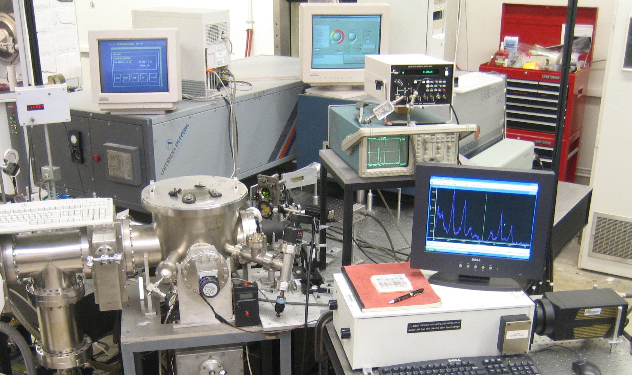
Dynamic plasma optical spectrum analysis
The in-situ optical plume diagnostic system located at LAMSAT can be used for two-dimensional time-resolved and/or time-integrated imaging and spectroscopic analysis (UV-Vis-NIR) of the emitted light from the laser-ablated plumes. The set up is equipped with Princeton Instruments Pi-Max high speed (< 5 ns) Intensified Charged Coupled Device (ICCD) camera with 512 x 512 pixels resolution.
This system can also be combined with the patented two-dimensional optical filter developed at LAMSAT for spectrally filtered imaging.
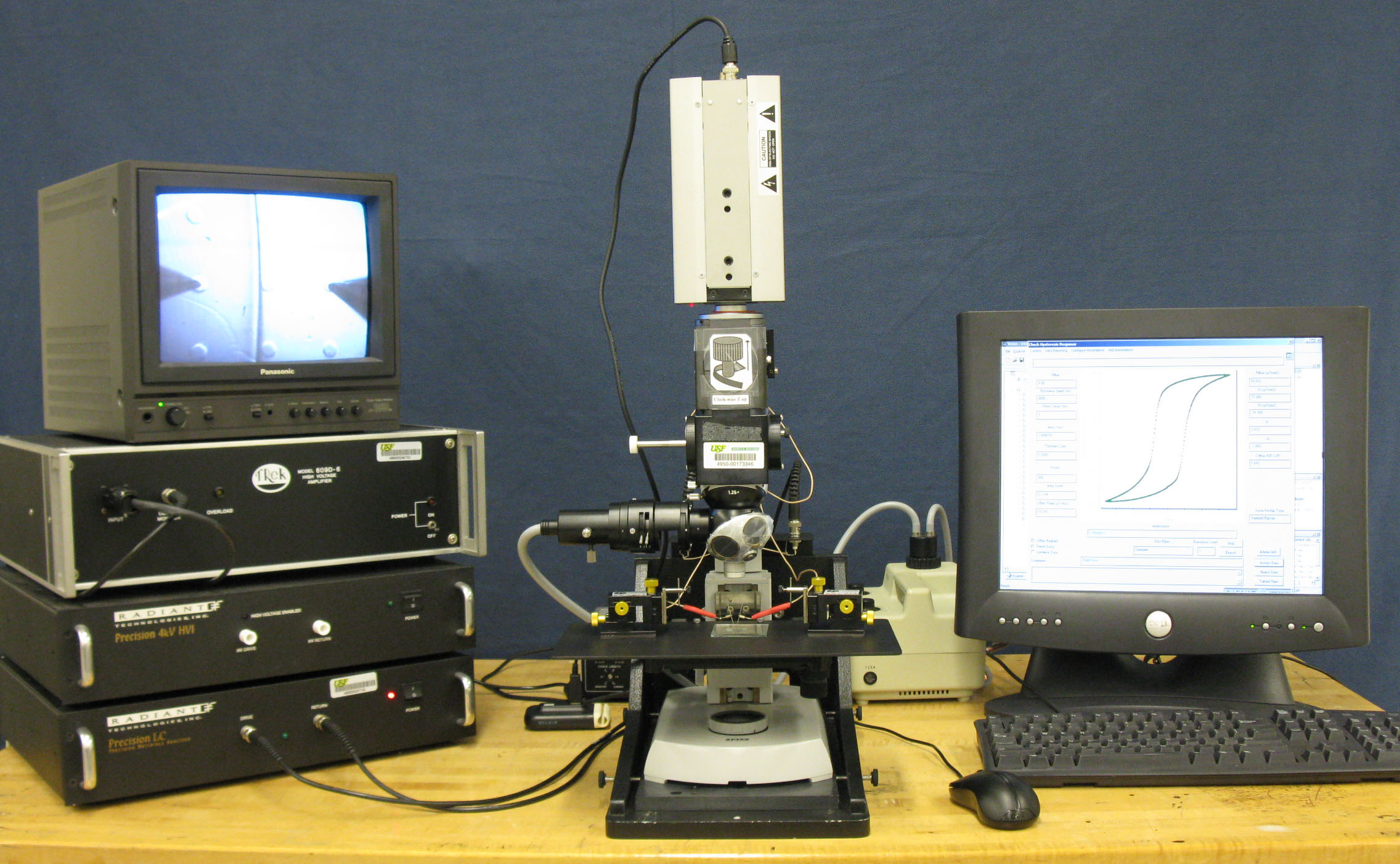
Ferroelectric tester
This instrument available at LAMSAT has been specially designed and assembled for measuring the ferroelectric properties of thin-films. The set-up consists of a Precision LC Materials Analyzer (ferroelectric tester), an optical microscope with video monitor, a probe station, and control PC. The Zeiss microscope is equipped with a video camera for monitoring microprobe position. The probe station includes sample stage holder, x-y-z micro-manipulators and pole pieces. The micro-manipulators on the probe station are KRN-01A 'DC' positioners from J-Micro Technology. In addition this system is also capable of I-V, C-V, leakage current, and resistivity measurements.
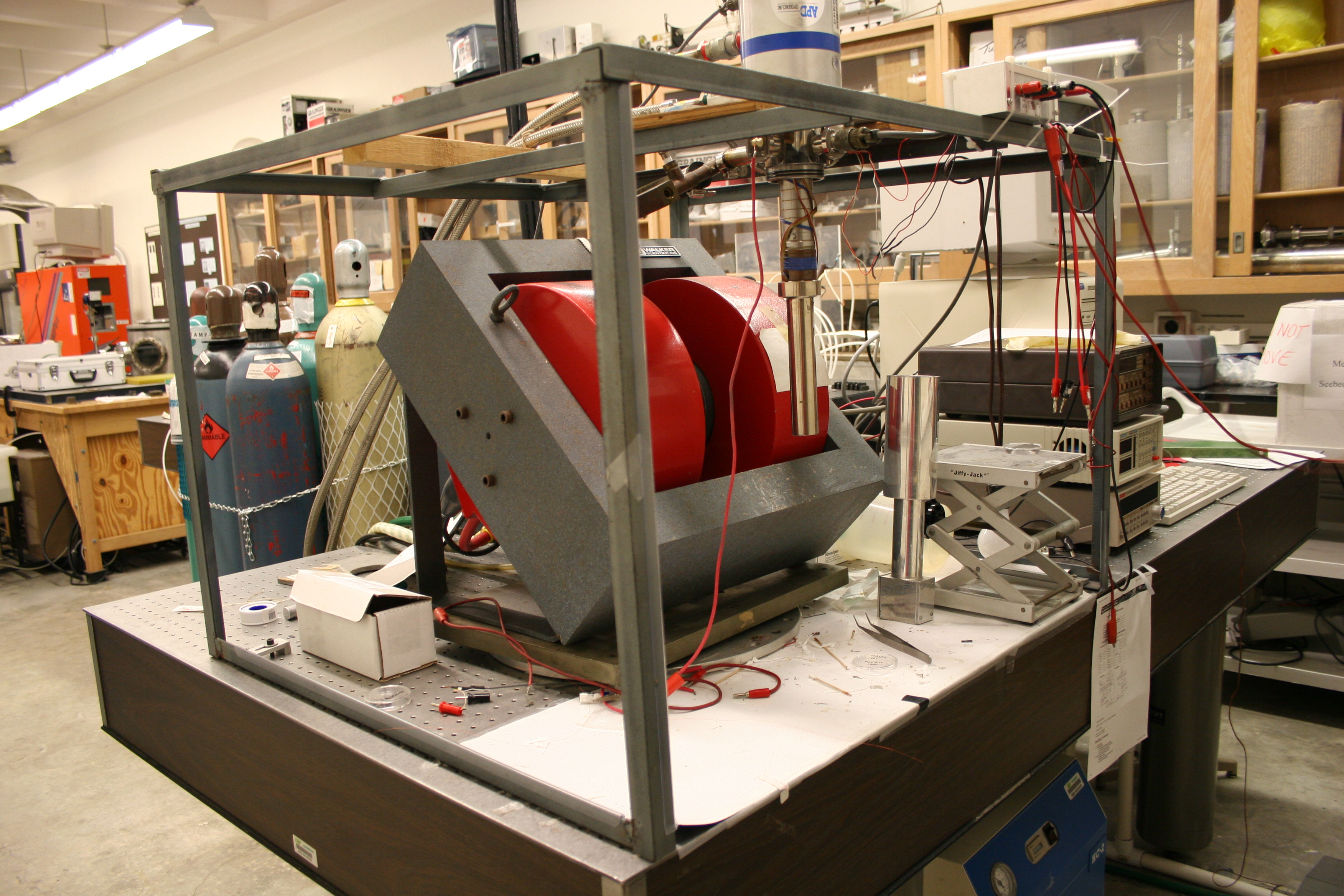
Hall Effect measurement system
The Hall Effect and resistivity measurement system available at LAMSAT is used for electrical characterization of thin films. The computer controlled system is equipped with a compressed He cryostat which can be cooled to 15 K for performing temperature-dependent measurements.
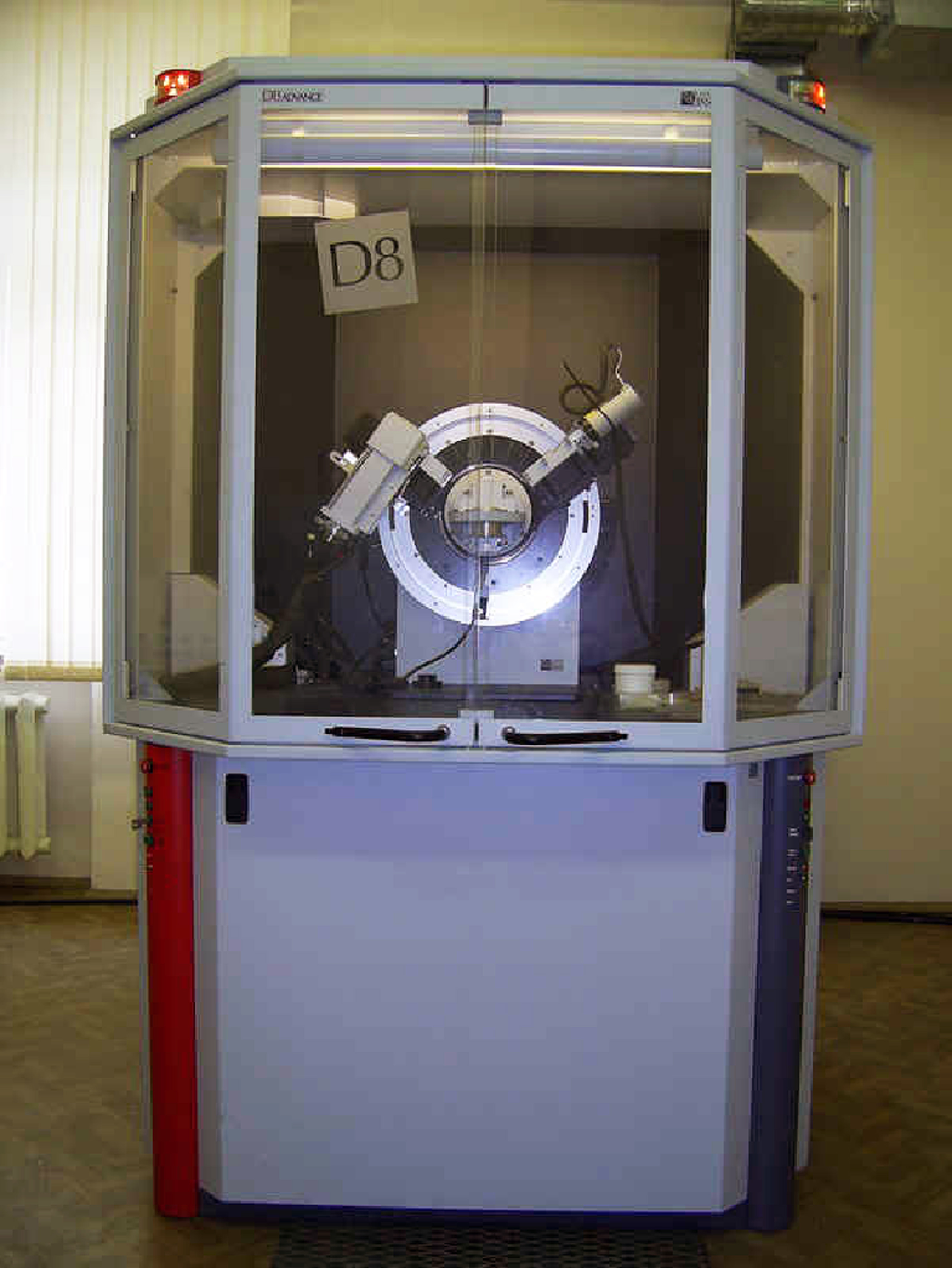
XRD
LAMSAT members have access to equipment in the Physics Materials Diagnostic Facility (PMDF) which includes a Bruker D8 Focus X-ray Diffractometer (XRD). The XRD is used for structural characterization such as the crystallinity of thin films, including lattice parameters, identification of unknown materials, orientations of single crystalline films, preferred orientations of polycrystalline films, defects, stress, etc. The system can perform all linear scans such as θ-2θ scans, 2θ-ω, asymmetric or detector scans, and rocking curves.
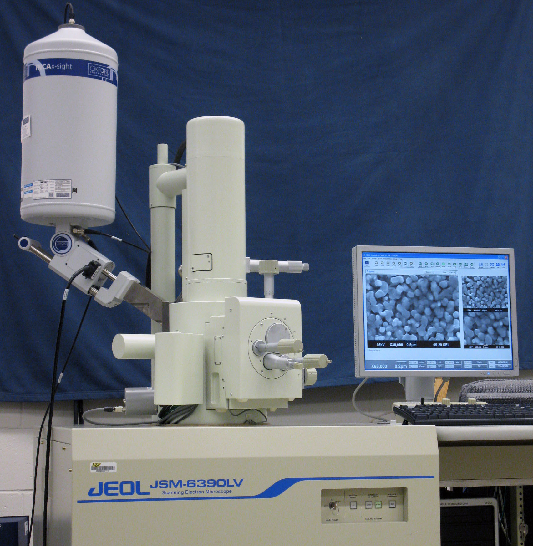
SEM with EDS
LAMSAT members have access to equipment in the PMDF which also includes a tungsten filnament JEOL JSM-6390LV Scanning Electron Microscope (SEM). The microscope is equipped with secondary electron imaging (SEI) and backscattered electron imaging (BEIW) detectors for compositional contrast, topographical, and shadow imaging. The SEM is used to characterize the surface morphology of thin films, powders, and biological samples. The SEM has a maximum resolution power of 3 nm at an acceleration voltage of 30 kV. The magnification could be varied from 5x to 300,000x. It is also equipped with an energy dispersive spectroscopy (EDS) detector from Oxford Instruments INCA x-sight for compositional analysis.
Typical applications include:
• Imaging surface morphology of thin films and powders
• Cross-section imaging of multilayer thin films or nanocolumn coatings
• Composition of powders and thin films
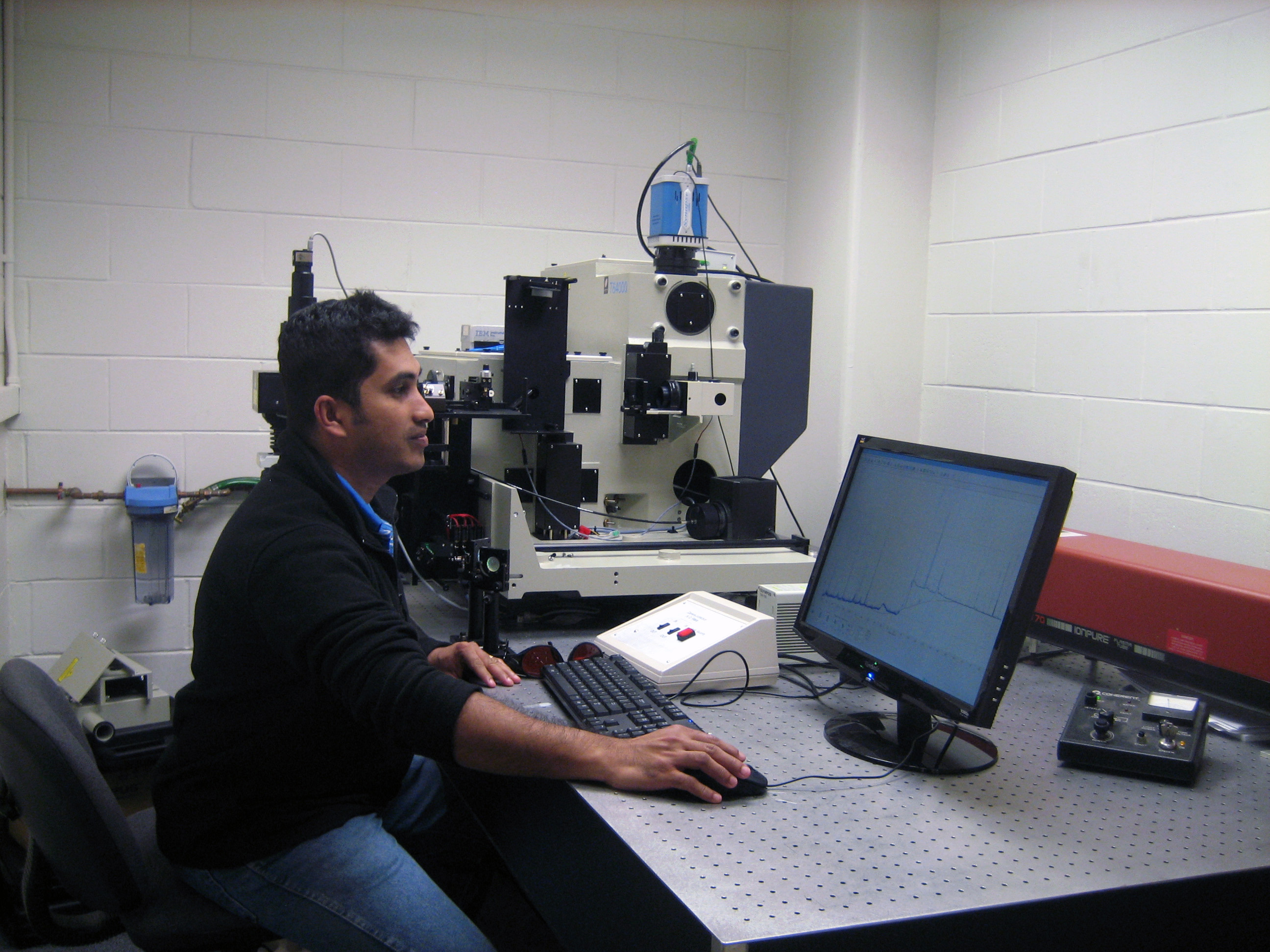
Triple spectrometer Raman system
The T64000 system is designed to provide a versatile platform for Raman analysis. It has an integrated triple spectrometer design for unprecedented optical stability. The instrument incorporates the proven technology of the confocal LabRAM Raman microprobe. The mechanical coupling is rigid and stable. The optical coupling is efficient and throughput is limited only by theoretical considerations. The main features are:
• High stray light rejection
In using the double subtractive configuration of the T64000, it is possible to obtain spectral information very close in to the laser line. The subtractive mode is ideal for studying such detail as crystal lattice modes.
• Ultra high resolution
With the use of the ultra-high resolution triple additive configuration of the T64000 triple system, it is possible to very accurately study the position of Raman bands.
• Single spectrometer
With the final mode of operation, the direct spectrograph entrance, the system can be used with holographic notch filter technology and as a more conventional single spectrometer based system. The high throughput of the large optical components means that it is then ideal for Raman mapping and even remote probe forms of analysis.
• UV Raman Spectroscopy
The high stray light rejection enables lower frequency Raman bands below 100cm-1 to be observed even in the deep UV (244nm). It can provide a complete spectral analysis not limited in its scope or range.
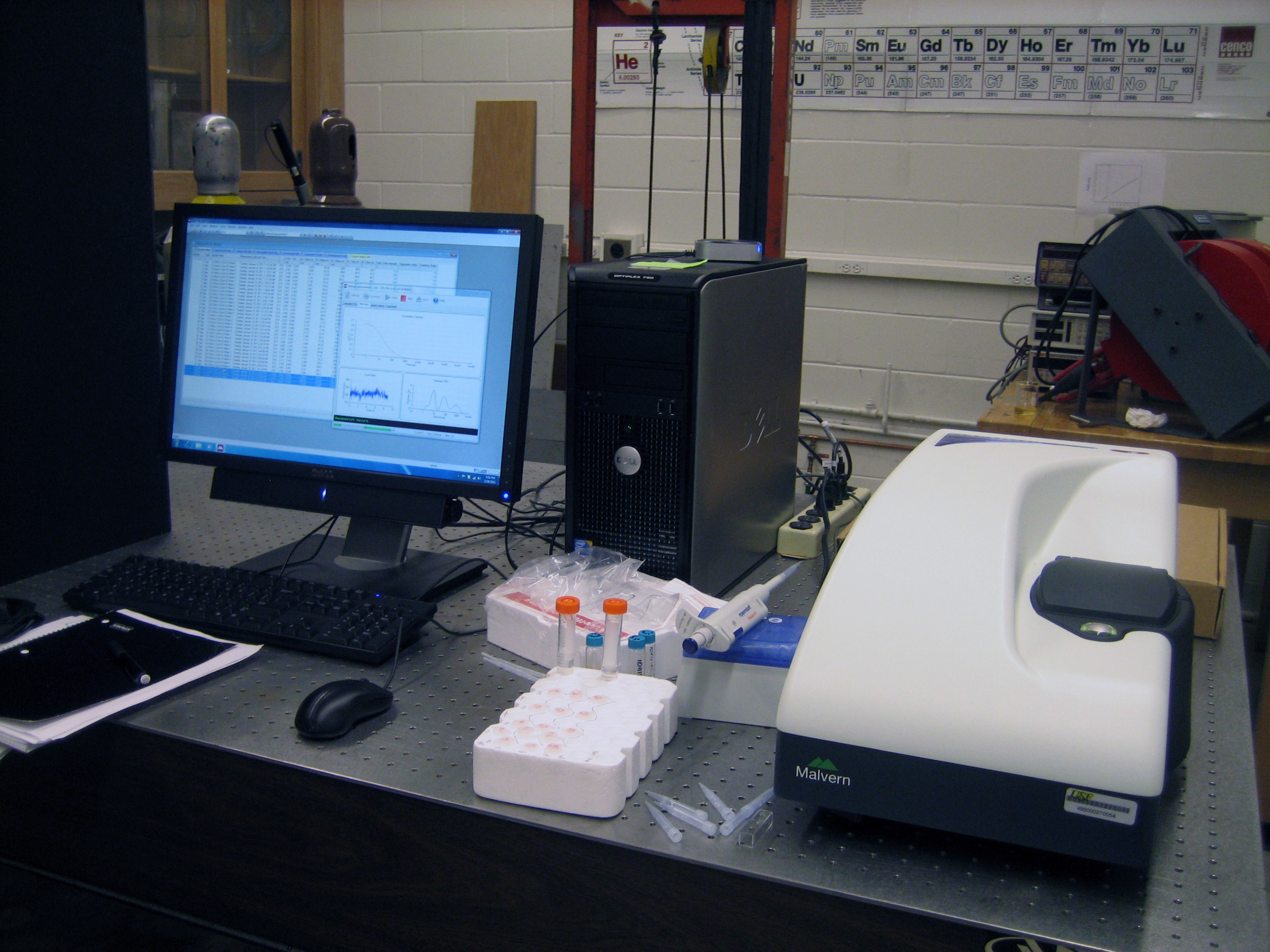
Zetasizer Nano S
Malvern Instruments' Zetasizer Nano series can measure:
• Particle size
Non-invasive back scatter (NIBS®) technology takes particle sizing to new levels of sensitivity in the 0.6nm to 10
micron range. The new Zetasizer Nano-S is the choice for the accurate, reliable and repeatable size analysis of particles and molecules in solution.
• Molecular weight
Using static light scattering (SLS) and the classical Debye plot, the molecular weight of random coiled polymers up to 5 x 10⁵ Da as well as globular polymers and proteins up to 2 x 10⁷ Da can be determined without the necessity for multi-angle measurements.